
Log in to iLab to see the schedule and availability or email Dr. Julian Sabisch (jsabisch@ou.edu) for a consultation.
The TEM Capabilities document (PDF) provides a graphical overview our TEM capabilities.
We're happy to answer any questions and work with you to acquire new caapabilities.
Located in GLCH room 38 (basement) | Availability
Transmission electron microscopy examines structure by passing electrons through the specimen. The image is formed as a shadow of the specimen on a phosphorescent screen. In order for electrons to pass through the specimen, it must be very thin (usually less than 100 nanometers or approx. 1/25,000 inch) thick. High resolution samples must be at least 1/5 this thickness to approach the resolution that this microscope is capable of. Specimen preparation requires considerable precision equipment, time and skill. TEM is typically used to examine the internal organization of objects of many kinds, but typically extremely thin and very clean. The JEOL 2010F is used for nanotechnology applications requiring higher resolution than the JEOL 2000 and Zeiss 10. Clean specimens and high-resolution imaging methods must be used to optimize samples.

High resolution is available for a wide range of samples, after appropriate sample prep with new Fishionne ion milling systems. Tto see atomic comlums requires minimal sample thickness; for best results samples must be below 20nm in total thickness, with minimal defects induced by the thinning process. Chemical and crystallographic characterization is also available, as well as our cyrogenic holder, which reduces the thermal noise in samples for higher qualty characterization.
High resolution transmission electron imaging typically requires a field emission source, a high accelerating voltage, and a thin crystalline specimen often only a few atomic layers thick, but achievable up to a few tens of nanometers. This can be achieved through a variety of methods, including grinding or etching a sample to several micrometers in thickness and then bombarding them with an ion beam to remove atoms one by one, using the imparted energy of the ion to displace an atom until the correct thickness is achieved. Our STEM is currently limited to ~2nm resolution, however we are developing our ability for STEM imaging down to the microscope's ultimate resoltuion. TEM imaging has been characterized down to 1Å resolution.
Below is a Si(110) crystal often used as an ideal specimen to characterize a non-aberration corrected microscope's resolution capabilities . The raw image (below) shows the so-called silicon dumbbells characteristic of this material. This image was taken with no noise in the building at 5 am
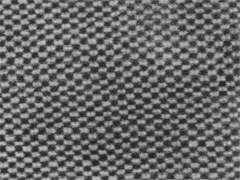
The image was then Fourier filtered to remove random noise and enhance contrast arising from the periodic elements. Thus, aspects of the crystal structure can be directly observed and measured.
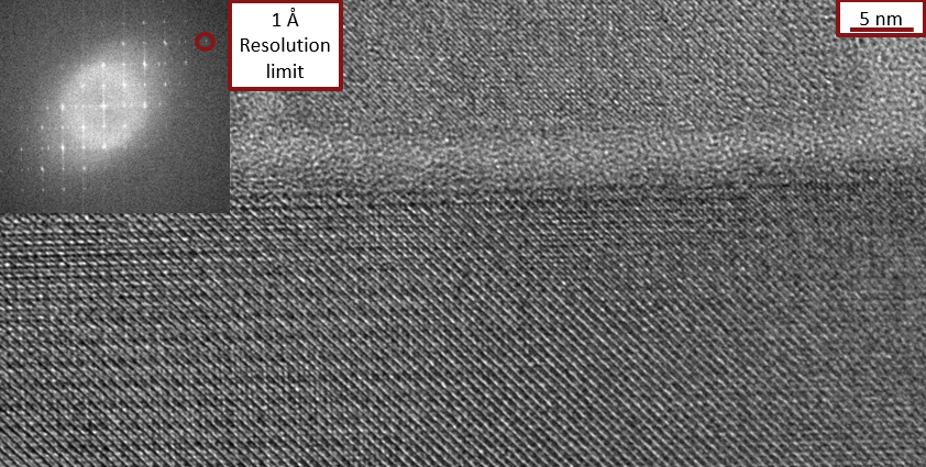
High Resolution TEM imaging is the most readily available and highest resolution imaging available on the 2010F. Unlike HR-STEM images, HR-TEM images must be simulated in order to fully understand the structure (please contact Dr. Julian Sabisch for TEM simulations). Below is an example TEM image showing a CsPbBr3 Perovskite structure with inset Fourier transform, showing an ultimate resolution of 1Å. With the new AMT camera, both diffraction patterns and better signal-to-noise imaging is available, to push the characterization of nanostructures further than previously possible.
Located in SLSRC room 1655 (NE corner) | Availability
The ThermoFisher FEI Tundra 100kV Cryo-TEM used for single particle cryo TEM grid analysis and screening. Located in the Stephenson Life Science Research Center (SLSRC), this electron microscope will be vital in expanding the scope of structural Biology research at OU.
The nearby Biomolecular Structure Core can assist in the preparation of grids for the collection of cryo-EM single particle analysis (SPA) data. The facility has a Pelco easiGlow discharge system for grid preparation and a Leica EM-GP2 cryo plunger as well as a ThermoFisher Vitrobot for freezing samples. An assortment of commonly used cryo-EM grids is available in the BSC. The BSC can assist with shipping of samples to cryo-EM data collection facilities, as well as data transfer and processing. Individual researchers will need to apply for data collection time for their projects at a national cryo-EM center.
The cryoplungers and glow discharger are located in room 2750 of the Stephenson Life Sciences Research Center on the University of Oklahoma-Norman Research Campus.
Scheduling for the use of the grid preparation equipment can be done by contacting the facility director, Dr. Len Thomas, lmthomas@ou.edu, (405) 325-1126.
In collaboration the BSC, SRNML can assist in screening of cryo-EM grids and data collection on OU’s ThermoFisher FEI Tundra 100 kV Single Particle Cryo-TEM.
Please contact the BSC facility director, Dr. Len Thomas, lmthomas@ou.edu, (405) 325-1126 or the SRNML TEM specialist, Dr. Julian Sabisch, jsabisch@ou.edu for more information.
Applicable fees will be charged for equipment training, use, and services: grid/sample preparation fees and Tundra usage fees.
Funding for the instrumentation was provided, in part, by an Institutional Development Award (IDeA) from the NIH (Award P20GM103640 and P30GM145423, PI: Dr. Ann West).

Located in GLCH room 221 (2nd floor hallway by elevators) | Availability
Transmission electron microscopy examines structures by passing electrons through the specimen. The image is formed as a shadow of the specimen on a phosphorescent screen. In order for electrons to pass through the specimen, it must be very thin (usually less than 100 nanometers or approx. 1/25,000 inch) thick. This requires considerable preparation equipment, time and skill, all available upon request at SRNML. TEM is typically used to examine the internal structure of nanomaterials, as electrons interact with specimen as they pass through. The JEOL 2000 is used for materials sciences applications and biological applications requiring ambient temperature and relatively low (for TEM) resolutions. It is a stable workhorse microscope that is quite flexible for TEM and X-ray spectroscopy as well as easy and quick to use. In addtion, it has a Gatan (1024 x 1024) scintillator coupled CCD camera installed.

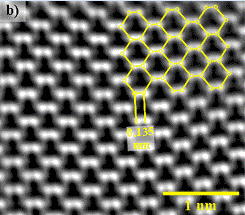
Below is an example HTREM image of a CsPbBr3 perovskite showing an ultimate resolution of 3Å.

To be located in Lin Hall B21
More details soon!
