The condensed matter group encompasses semiconductor physics, soft-matter physics, and nanophysics. A major focus of our group is the experimental and theoretical study of highly confined electron systems in artificially structured semiconductors and other low dimensional materials. We cover all aspects of these systems from fundamental theory to device fabrication. We have theoretical and experimental efforts in nano-scale semiconductor devices, high-efficiency photovoltaics, graphene, self-assembled monolayers, and nanoparticles. Some of this work is performed in conjunction with researchers in the Departments of Chemistry and Biochemistry, Electrical & Computer Engineering, and Chemical, Biological, & Materials Engineering.
The faculty in condensed matter physics share appointments in the engineering physics program. The engineering physicist provides the link between the pure scientist and the engineer by applying fundamental scientific theories to the solution of technological problems. As the miniaturization of transistors, lasers, and memory elements continues, an understanding of their operation increasingly requires knowledge of the underlying physics. The group has several long-standing collaborations with National and International partners including the Naval Research Laboratory, SUNY Buffalo, the University of Tulsa, Oklahoma State University, Virginia Tech, University College London, CRHEA-CNRS in France, Tohoku University in Japan, and with Industrial partners at Amethyst Research Inc. and IBM, amongst others. The Sellers group is also an active member in the Oklahoma Photovoltaics Research Institute, a consortium of academic and industrial groups from around the state focused on developing collaborative research and education programs in photovoltaics research.
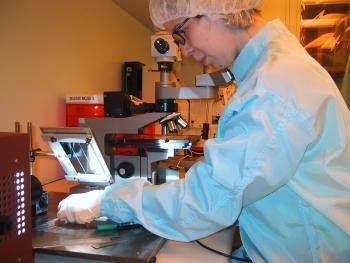
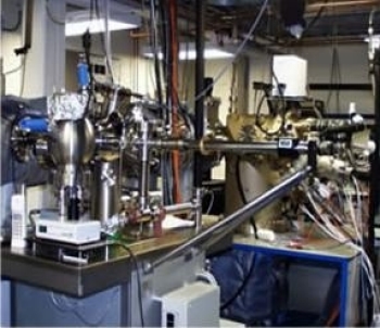
The majority of our experimental research takes place in the department’s state-of-the-art laboratories. Our well-equipped facilities include: a dual-chamber molecular beam epitaxy (MBE) system for the growth of III-V semiconductors; several scanning tunneling and atomic force microscopes for high resolution imaging and patterning of atomic surfaces; a cleanroom for optical lithography and semiconductor processing; a thin-film laboratory for routine vapor deposition; variable temperature (4-300 K) and high magnetic field (7 T) facilities for magneto-optical studies; optical microscopes for single nanoparticle spectroscopy; a grazing angle infrared spectrometer for molecular spectroscopy of monolayers; and full characterization techniques for solar cells analysis including a class-A solar simulator, an external quantum efficiency system with capacitance-voltage analysis equipment. Scanning electron and transmission electron microscopes are available in the Samuel Roberts Noble Electron Microscopy Laboratory and are routinely used by our students for their research.
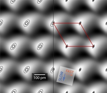
Lloyd Bumm is working to achieve new insights to the structure and motion of molecular films at the picometer scale with our ultra-stable scanning tunneling microscope (STM). The advanced real-space image analysis techniques we are pioneering are combined with molecular dynamic simulations for a unique understanding of the molecular environment. Molecular films are commonly used to modify the chemical and physical properties of surface. Increasing they are used as interfacial modifiers in nanomaterials for environmental passivation and electronic band alignment. Our studies are performed under near ambient conditions to approximate real world environment. The goal is to understand the role of intrinsic molecular motion and surface defects on the properties of practical surfaces. The understanding we gain is critical for engineering surfaces with better environmental stability or surfaces with planned failure modes.
Ian Sellers performs work on novel structures for high efficiency next generation solar cells and for space power generation. Specific projects involve a fundamental analysis of quantum structures and architectures that provide the potential to harness more of the available solar energy, and projects to assess the radiation hardness and thermal stability of thin film solar cells for deep space missions. The Sellers’ group is also a leading participant in the Oklahoma Photovoltaics Research Institute, collaborates closely with National Laboratories, and several University groups worldwide.
Kieran Mullen and Bruno Uchoa are interested in many areas of research including new quantum phases in strongly correlated systems, quantum criticality and transport in semiconductor and carbon nanoscale systems.
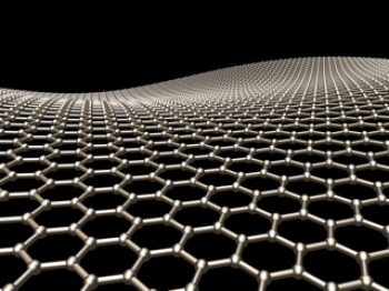
New quantum states of matter have been found in a variety of materials in which the electronic many-body states are protected by topology. Many of these materials have elementary electronic quasiparticles that behave as Dirac fermions, the relativistic analogs to massless neutrinos. This class of electronic systems is called “Dirac materials” and current examples include graphene, (a new 2 dimensional allotropic form of carbon), topological insulators, and Weyl semimetals. Other novel correlated states can be found in semiconductor nanostructures that have no simple atomic analog, such as in rings or spherical shells. New quantum phases include chiral edge states in topological insulators, novel superconducting condensates in carbon-based systems, and polarized arrays of quantum rings.
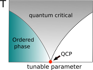
Quantum criticality refers to phase transitions driven by quantum fluctuations rather than temperature. It is unusual in that quantum mechanics can be made manifest on a macroscopic level by tuning the system through its quantum phase transition. Examples of candidate materials for the experimental observation of quantum criticality include high temperature superconductors, heavy fermions, Dirac materials among other systems.
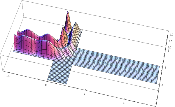
Transport on the nanoscale can be profoundly different from classical transport. Our studies involve currents in heat, charge, energy, spin and pseudospin in mesoscopic systems in general. We have predicted diverse transport results ranging from supercurrents in stressed graphene monolayers to cooling of an electron gas by “blowing off” the hotter parts of the current . Areas of interest include the role of disorder and many body effects into transport. In addition theory is an important partner to the experimental efforts of the Condensed Matter group.