Log into iLab to see the schedule and availability, or email Dr. Preston Larson (plarson@ou.edu) for questions and consultations regarding SEM.
The SEM Capabilities document (PDF) provides a graphical overview of our SEM capabilities.
We're happy to answer any questions and work with you to acquire new caapabilities.
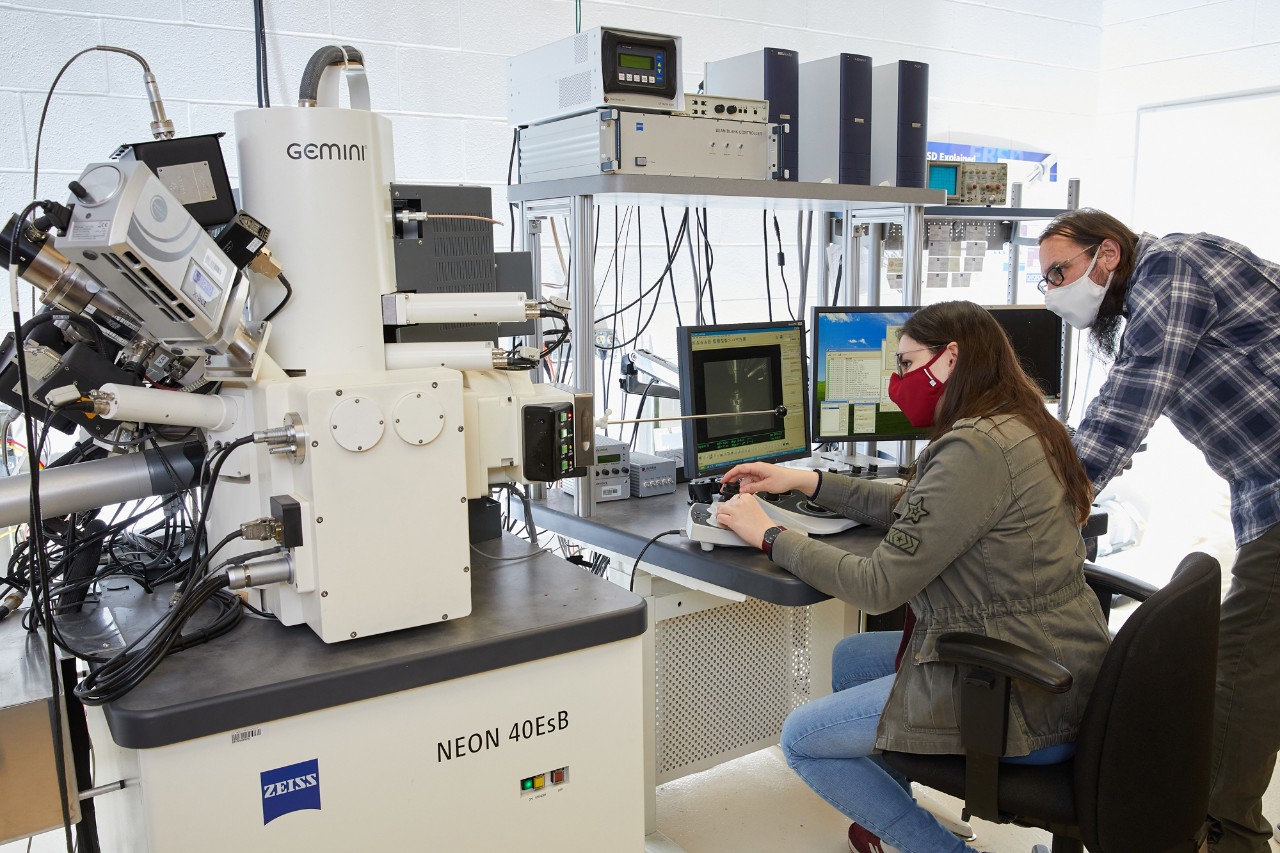
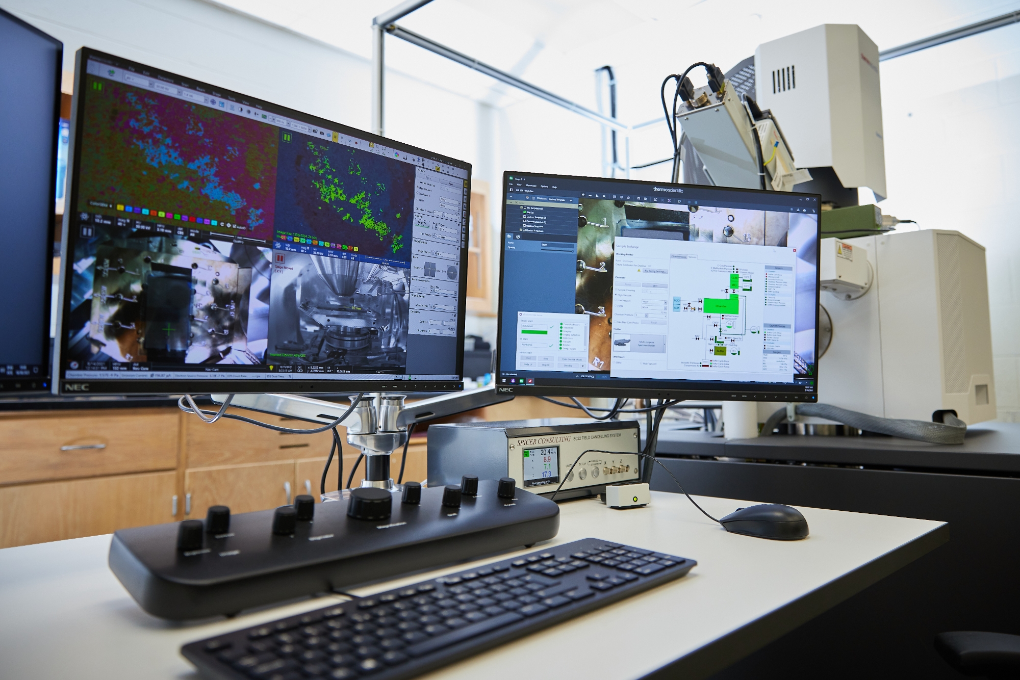
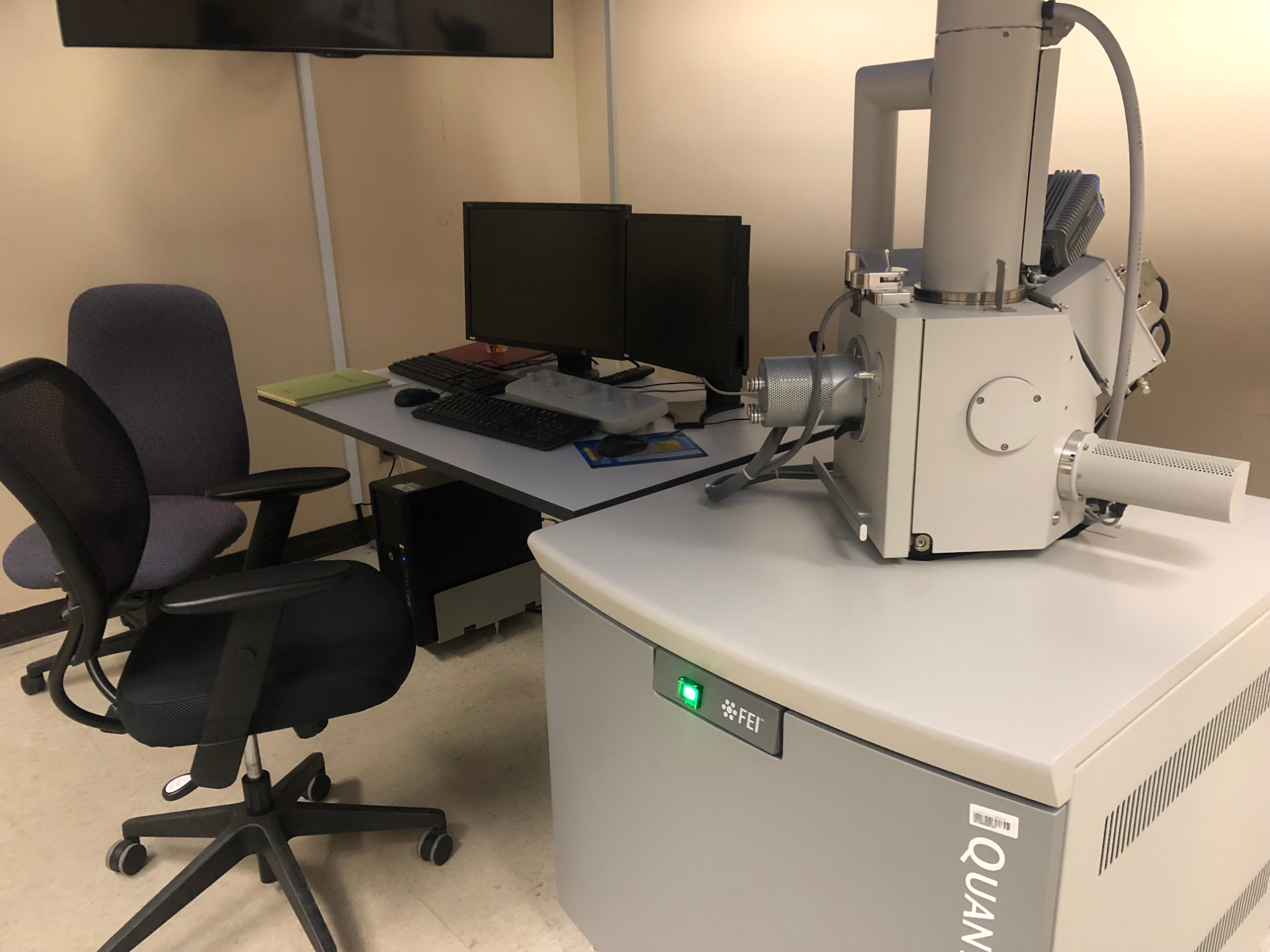
Located in GLCH room 48 (basement) | ThermoFisher Quattro S Availability
Our ThermoFisher Quattro S is a versatile platform for imaging and analysis
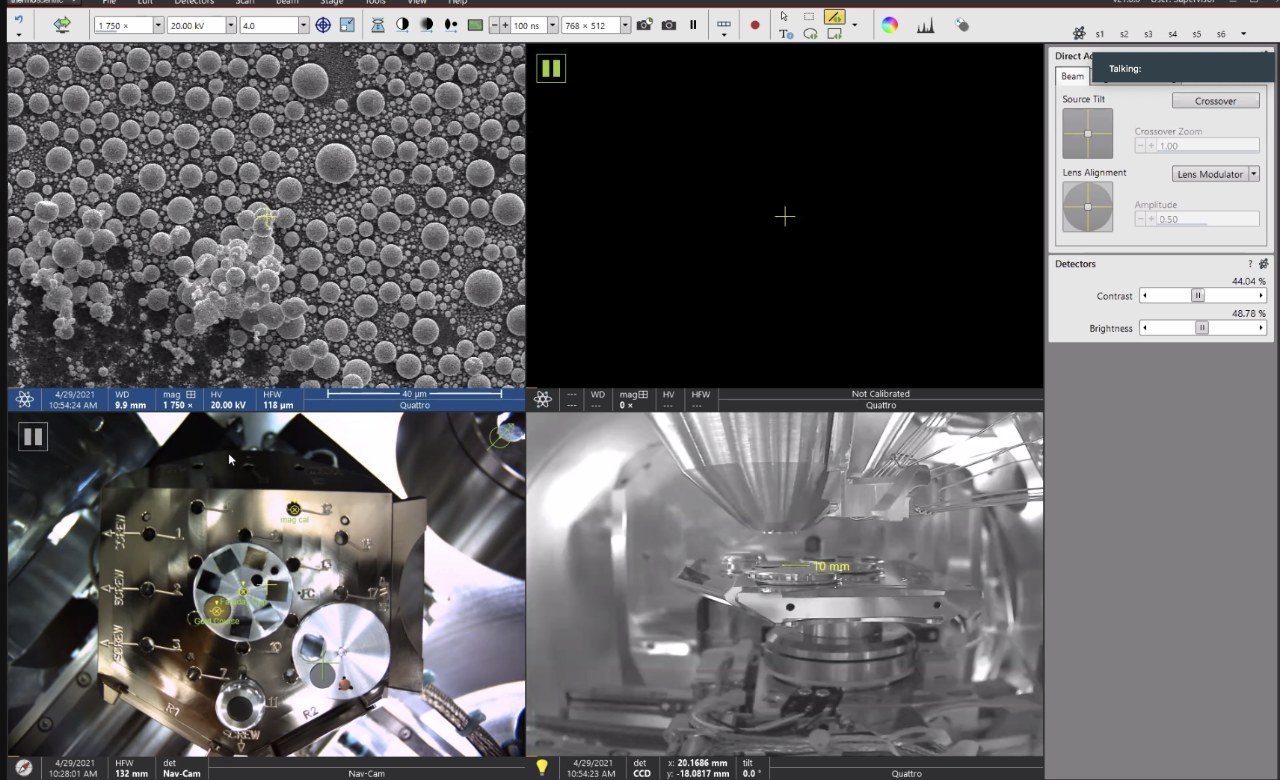
Located in GLCH room 18 (basement) | Zeiss NEON 40 EsB Availability
The Zeiss NEON 40 EsB combines the imaging and analytical capabilities of a high resolution FE-SEM, using the proven GEMINI lens design, with an advanced Canion FIB column. In addition, this CrossBeam system has a multi-channel gas injection system (GIS) for deposition of metal and insulating layers, and can also perform enhanced and selective etching. The EsB (integrated energy and angle selective BSE) detector of the NEON 40 provides advanced compositional information and ultra-high BSE imaging at very short working distances. Other features include a 6-axes fully eucentric motorized stage, IR CCD camera for sample viewing, 100mm airlock, and integrated CrossBeam/SmartSEM GUI.
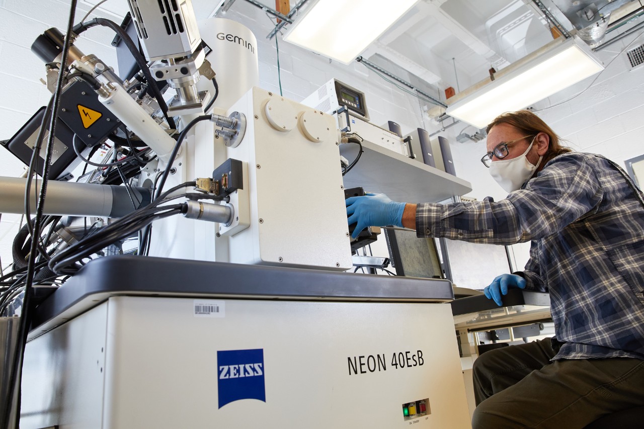
This microscope is the most capable of the SEMs that we own. It is useful for many specialized purposes, including being able to section materials in realtime, deposit materials, erode materials, conduct electron tomographic reconstructions, as well as high resolution scanning electron microscopy.
Located in Sarkeys Energy Center (SEC) E218 | AFEI/TFS Quanta Scanning Electron Microscope Availability
Intstrument scientist: Dr. Preston Larson
Located in NML 205 | Hitachi TM3000 Availability
The most special feature of this scanning electron microscope is that it is truly a tabletop SEM, it is portable and it is designed for minimal preparation of specimens. The microscope is lightweight by design, using a diaphragm pump instead of a rotary pump and a turbomolecular pump instead of a diffusion pump to achieve a useful vacuum for observation. Also the vacuum is on the low side, so it is a semi-environmental SEM and quite tolerant of moisture (unlike any of our other electron microscopes!). The SEM functions by a touch screen and features automated astigmation, focusing, start up and alignment. The TM3000 is a serious SEM but with a simple enough interface to allow its use in the classroom. The HITACHI TM3000 is used for normal sized specimens. There is no airlock. Specimens are mounted on a specialized holder adjusted in height to optimize operation and the SEM is then pumped down until the green progress bar indicates that the microscope is ready. A serious use for this instrument is screening plant and insect mutants in genetic studies where rapidity of specimen exchange is needed and high resolution is not. Minimal specimen preparation is required because the imaging mode used is tolerant of moisture and charging.
This microscope joined the lab in 2010 and is used for demos, quick examination of genetic mutants, student projects and a myriad of samples needing a quick "look see".
The HITACHI TM3000 is a specialized SEM that uses mainly backscattered electrons to image the specimen, rather than secondary electrons, which require a better vacuum. This is called "charge reduction mode by Hitachi" and means that to prevent charging, that contaminants are tolerated to a greater degree in this particular SEM than the more expensive SEMs that operate in a higher vacuum environment. The screens below show the controls, which are all virtual (except for the two specimen movement knobs and the pump button) and are located on the computer screen. The microscope is controlled by a touchscreen or a mouse, at the user's choice. It is well designed and a hit at Oklahoma Uglybug Contest Award assemblies in the schools!
The HITACHI TM3000 accepts conventionally-sized specimens but it does not normally use stubs. Instead the materials are mounted directly to the specimen holder, which is adjusted to the appropriate height for focus using a height adjustment screw. No coating is necessary since charge compensation is used to dissipate charge accumulation as electrons bombard the specimen.